The Compounding Cost of Defects
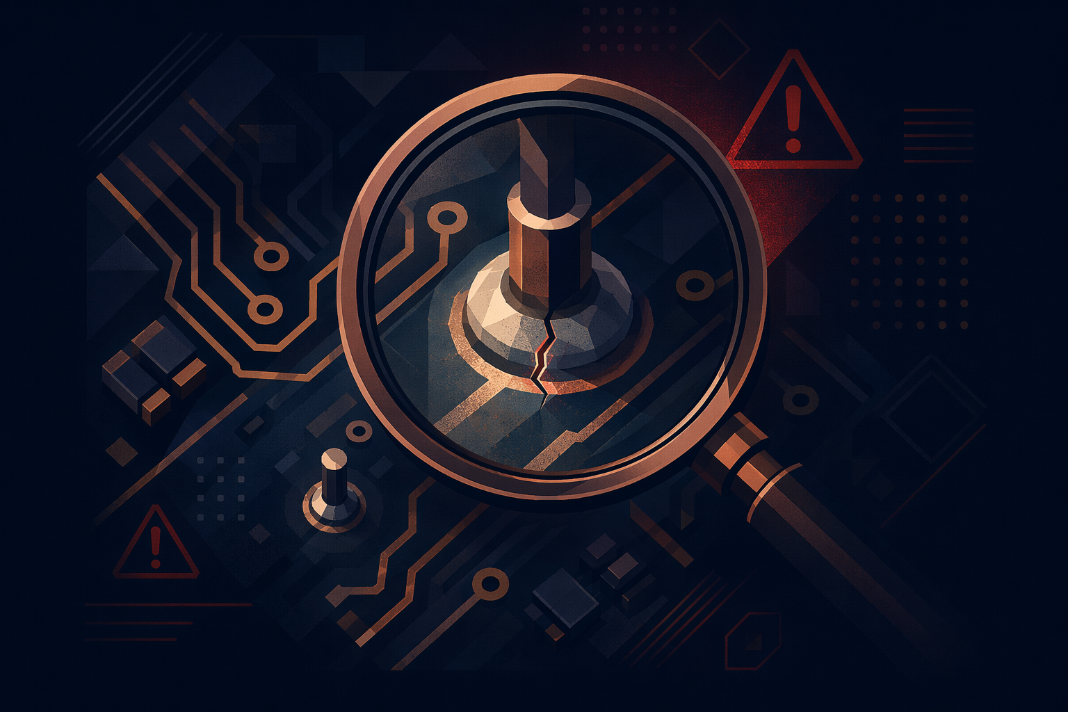
There is a well-known rule of thumb in electronics manufacturing: a defect that costs one dollar to catch at the fabrication stage costs ten dollars to catch during assembly, and one hundred dollars to catch in the field. The numbers are not hyperbole — they come from decades of cost-of-quality data aggregated across automotive, aerospace, and medical device supply chains. A solder bridge discovered at AOI costs the time of a rework technician and a few grams of solder. A solder bridge discovered after the product ships to a customer costs a field service visit, a replacement unit, shipping both ways, engineering root-cause-analysis time, and potentially reputational damage that no line item can capture.
The cost multiplier is not linear because the consequences compound. A field failure triggers investigation of the entire production lot, containment measures, corrective action reports, and possibly regulatory notification — all before you have even paid for the physical repair. This is why inspection is not a cost center. It is an insurance policy with a near-immediate return.
Common Defect Types in PCB Assembly
The defects that escape a line without adequate inspection fall into predictable categories. Most are preventable with the right combination of process control and detection technology.
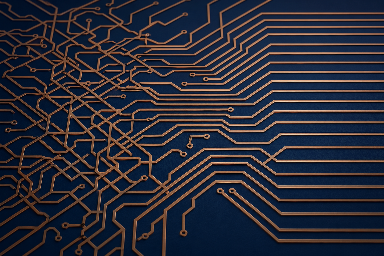
- Solder bridges: Unintended solder connections between adjacent pads or leads, most common on fine-pitch QFPs and 0201/0402 passives. Causes range from excessive paste deposit to stencil misalignment.
- Insufficient solder: Joints with inadequate solder volume, risking intermittent opens under thermal cycling or vibration. Often traced to partially clogged stencil apertures or insufficient squeegee pressure.
- Tombstoning: One end of a chip component lifts off the pad during reflow, standing vertically like a tombstone. Caused by uneven wetting forces, typically from pad geometry asymmetry or temperature imbalance across the component.
- Component shift: Parts that move during reflow due to unbalanced solder surface tension or insufficient tack force from the paste. Fine-pitch QFNs and BGAs are especially susceptible because their small mass offers little resistance to surface-tension-driven movement.
Inspection Technologies and Where They Fit
No single inspection method catches everything. A robust quality system uses a layered approach where each technology compensates for the limitations of the others.
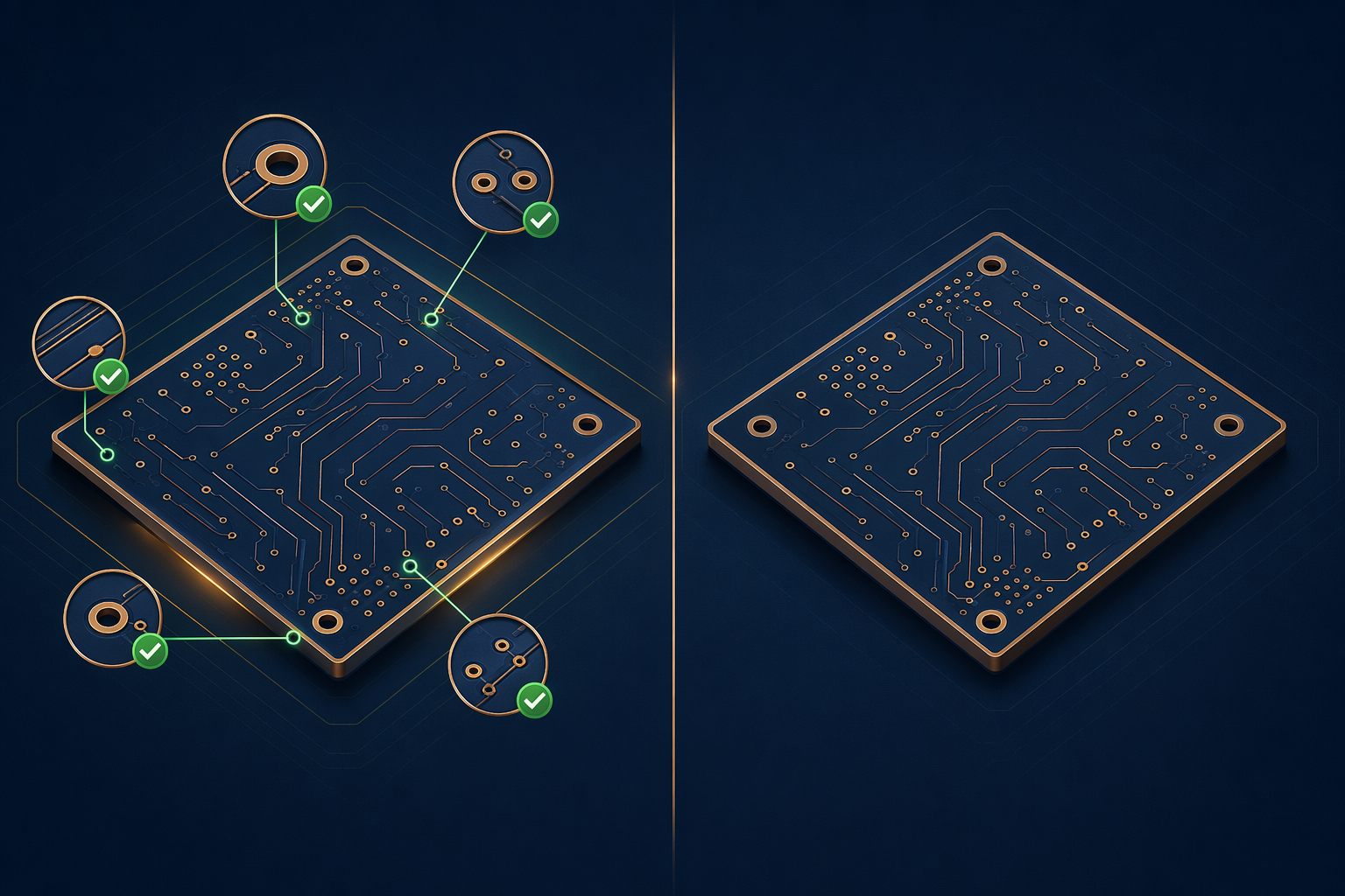
Automated Optical Inspection (AOI) uses high-resolution cameras and multi-angle lighting to compare every joint on every board against a golden reference image. It excels at finding solder bridges, insufficient solder, missing components, and polarity errors. AOI is fast — it keeps pace with the line — and it is the first gate every board should pass after reflow. Its limitation is that it cannot see under BGAs, inside PTH barrels below the surface, or through components to hidden joints.
X-Ray Inspection (AXI) fills that gap. It penetrates component bodies and solder joints to reveal voiding, insufficient ball collapse on BGAs, and hidden bridging under packages. Because it is slower than AOI, it is typically used for sampling on Class 2 builds and 100% on Class 3 builds with hidden-joint packages. In-Circuit Testing (ICT) and Flying Probe verify electrical connectivity — resistance, capacitance, diode polarity, short/open detection — by physically probing test points. They catch assembly errors that create electrically measurable faults but are invisible to optical inspection. Finally, Functional Test powers up the board and verifies that it performs its intended function under conditions that simulate real-world operation.
The ROI of Inspection
Investing in inspection yields direct, measurable savings. A single uncaught solder bridge on a BGA in a medical device can trigger a lot-level recall costing upwards of $50,000 in documentation, re-inspection, rework labor, and shipping — before any regulatory fines. AOI equipment amortizes over tens of thousands of boards; the per-board cost of inspection on a mid-volume line is typically under $2, while the cost of one field return can exceed $500 after shipping, engineering analysis, and rework.
Uppcba's Quality Approach
Every board assembled on our line passes through 100% AOI after reflow, with X-ray sampling on all BGA and QFN placements. For Class 3 builds, X-ray coverage expands to 100% of hidden-joint packages. A functional test verifies the board performs to specification under power. This three-layer approach — optical, X-ray, electrical — is the reason our first-pass yield rate sits at 99.7%. It is not magic. It is simply the discipline of catching defects at the cheapest possible point in the value chain.
If your current assembler is not providing inspection data with every shipment — or worse, if you are discovering assembly defects during your own functional test — the economics are working against you. Let us show you what a properly inspected board looks like.