Every PCB assembly shipped without testing is a bet against physics. Solder paste printing, component placement, and reflow soldering are mechanical processes with real tolerances — and when tolerances stack up unfavorably, you get defects. The question is not whether to test. It is which testing methods catch the defects that matter for your product, at what cost, and at what point in the production process.
At a well-run PCB assembly operation, testing is not a single gate at the end of the line — it is a layered strategy. Each method covers a different class of defects, and the methods are chosen based on the product's required reliability level, production volume, and board complexity. A consumer IoT device with a $25 BOM cost and an expected 2-year lifespan needs a different testing strategy than a Class III medical device implant where a single field failure triggers an FDA adverse event report.
This article covers the five primary testing methods used in professional PCB assembly — what each detects, what each misses, the per-board cost impact, and how to decide which combination is right for your product. Data and thresholds are based on Uppcba's production floor in Shenzhen, where we process approximately 12,000 boards per week across prototype and mid-volume programs.
1. Solder Paste Inspection (SPI): The Test That Prevents Defects Before They Form
SPI is technically a process control step, not a board-level test — but it is the single highest-ROI inspection investment on an SMT line. SPI inspects the solder paste deposit immediately after printing and before components are placed. It measures paste volume, height, area, and registration accuracy on every pad, comparing each measurement against programmed tolerances.
Why does this matter before a single component is placed? Because roughly 60–70% of SMT soldering defects originate at the solder paste printing stage — insufficient paste, bridging between fine-pitch pads, or paste smearing caused by stencil wear. If you detect these at SPI, you clean the board and reprint. If you miss them, you place components, reflow the board, and discover the defects at AOI or ICT — by which point you are reworking an assembled board instead of a bare one. The rework cost difference is approximately 8–15×.
What SPI measures: Paste volume (target ±30% for standard pads, ±20% for fine-pitch), paste height, area coverage on pad, X/Y offset from pad center, and bridge detection between adjacent pads. Modern SPI systems (Koh Young aSPIre, CyberOptics SE3000) measure every pad on a board in under 15 seconds using Moiré interferometry — projecting a structured light pattern onto the paste deposit and computing height from the fringe pattern distortion.
What SPI does not detect: Component placement errors (it runs before placement), solder joint quality after reflow, electrical continuity, or component authenticity. SPI is a front-end gate — it prevents paste-related defects from reaching reflow. It does not replace post-reflow inspection.
Uppcba runs inline SPI on every SMT line — boards with paste defects exceeding tolerance are diverted before component placement, not after. This alone eliminates approximately 6–8% of post-reflow defects that would otherwise require rework or scrap.
2. Automated Optical Inspection (AOI): The Workhorse of Post-Reflow Testing
AOI is the most widely deployed post-reflow inspection method, and for good reason: it is fast (3–8 seconds per board side for a mid-complexity board), covers every visible feature on the board, and costs approximately $0.03–0.08 per board in equipment depreciation and operator time. For the vast majority of commercial and industrial PCBs, AOI is the primary defect detection gate.
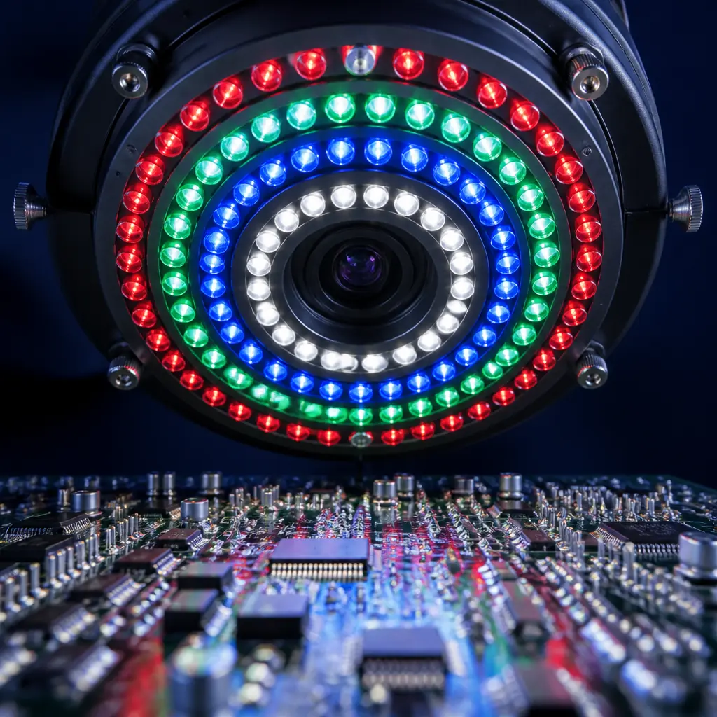
How AOI works: A high-resolution camera (typically 12–25 megapixel) with multi-angle lighting (top, side, and angled LEDs in red, green, blue, and white) captures images of every component and solder joint on the board. The system compares each image against a "golden board" reference or a CAD-derived template, flagging deviations in component presence, position, orientation, polarity, solder joint shape, and bridging. Modern AOI systems (Omron VT-S1080, Koh Young Zenith) use a combination of rule-based algorithms and deep learning models to reduce false-positive rates — a critical metric because every false positive requires a human operator to verify, and operator fatigue leads to real defects being missed.
What AOI detects reliably: Missing components, tombstoned components (one end lifted off the pad), billboarding (component standing vertically), wrong component polarity, solder bridges between adjacent pins, insufficient solder (less than 50% of expected fillet volume), and component offset beyond IPC tolerance (±25% of termination width for Class 2, ±20% for Class 3). In practice, AOI catches approximately 85–92% of visible solder defects on a well-programmed system.
What AOI misses: Anything it cannot see — and that is the entire category of hidden solder joints. BGA balls, QFN thermal pads, and the underside of J-lead packages are optically invisible after reflow. A BGA with 484 balls may have 483 perfectly soldered and one cold joint in the center — AOI sees the exterior balls and reports 100% pass while the intermittent open is waiting to fail in the field. For boards with any BGA, QFN, or LGA package, AOI alone is insufficient — you need X-ray.
3. X-Ray Inspection: The Only Way to See Hidden Solder Joints
X-ray inspection is the definitive method for evaluating solder joints under area-array packages — BGAs, QFNs, LGAs, and flip-chip devices. Optical methods cannot penetrate the package body or the PCB substrate to see the solder balls underneath. X-ray can, and for products where a single hidden open or short would cause a field failure with significant consequences (medical, aerospace, automotive safety), X-ray is not optional — it is a hard requirement specified in the quality plan.
2D vs 3D X-ray: A 2D X-ray system (transmission X-ray) produces a top-down image showing the density of material at each pixel — solder (high density, tin-lead or SAC alloy) appears darker, while the PCB substrate and component body (lower density, epoxy/FR-4/silicon) appear lighter. This is sufficient to detect solder bridges (shorts) between adjacent BGA balls and gross opens (missing solder) — the two most common BGA defect types. A 3D X-ray system (computed tomography, or CT X-ray) reconstructs a full volumetric model of each solder joint by capturing images at multiple angles, enabling measurement of void percentage, joint diameter, and standoff height. 3D X-ray adds approximately 3–5× to the equipment cost and 2–3× to the per-board inspection time compared to 2D.
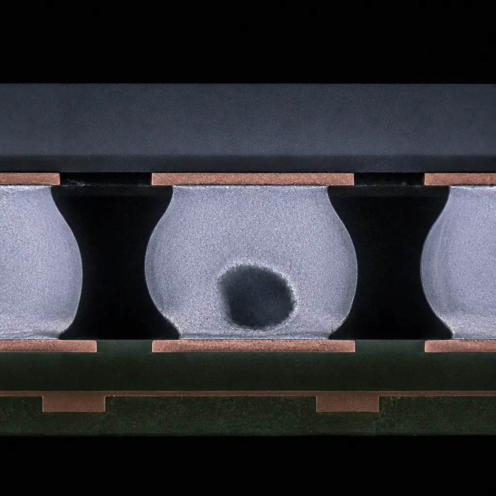
What X-ray detects that AOI cannot: BGA solder bridges (shorts between adjacent balls), BGA opens (balls that never formed a metallurgical bond with the pad), voiding percentage inside solder joints (IPC-A-610 Class 3 allows ≤25% void area per ball for BGA, ≤30% for PTH solder joints), and head-in-pillow defects (where the solder ball and solder paste both melted but did not coalesce — a particular risk with lead-free SAC alloys and moisture-exposed BGAs). Head-in-pillow is notoriously difficult to detect because the joint looks connected in 2D X-ray but has no actual metallurgical bond; 3D CT or oblique-angle 2D imaging with experienced operator interpretation is required.
Practical X-ray strategy for mid-volume production: For programs running 500–5,000 boards per batch, full-board 2D X-ray of every BGA/QFN site is achievable at roughly $0.25–0.50 per board in equipment cost. Uppcba's default quality plan includes 2D X-ray on 100% of area-array packages for all Class 3 programs, with 3D CT sampling (1 board per 100) to verify void levels and joint morphology. For Class 2 programs, X-ray sampling at 1 board per 50 is standard unless the client specifies a tighter requirement.
4. In-Circuit Testing (ICT) and Flying Probe: Electrical Verification
AOI and X-ray verify physical quality — solder joint formation, component placement, polarity. They do not verify that the circuit actually works electrically. For that, you need electrical testing: ICT or flying probe. These methods measure resistance, capacitance, inductance, diode forward voltage, transistor gain, and — critically — verify that every node in the netlist has continuity where it should and isolation where it should not.
In-Circuit Testing (ICT)
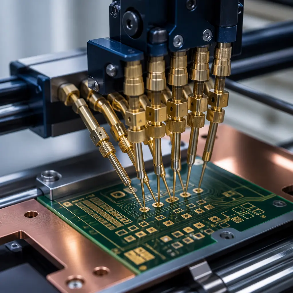
ICT uses a bed-of-nails fixture — a custom-machined plate with spring-loaded pogo pins that make simultaneous contact with test points on the bottom of the board. A test program sequentially powers each net, measures the component values, and compares them against programmed limits. ICT is fast: a mid-complexity board (200–400 nets) tests in 3–10 seconds. It is also comprehensive — a well-programmed ICT fixture catches open circuits, short circuits, wrong component values, wrong component orientation (for polarized parts), missing components, and manufacturing defects like insufficient solder on through-hole joints.
The cost tradeoff: ICT requires a custom fixture that costs $2,000–8,000 and takes 1–2 weeks to fabricate. This makes ICT economical for production volumes above roughly 200–500 boards — below that threshold, the fixture NRE dominates the per-board cost. For programs running 1,000+ boards per year, ICT typically adds $0.15–0.40 per board in amortized fixture cost plus operator time — and catches the kind of electrical defects that would otherwise require 10–30 minutes of bench debugging to isolate.
Flying Probe Testing
Flying probe uses 4–8 movable probes mounted on high-speed XY positioners that fly from test point to test point, making sequential measurements. No fixture is required — the test program is generated directly from the CAD netlist and Gerber files. This eliminates the fixture NRE entirely, making flying probe the default choice for prototype runs (5–100 boards) and low-volume production where fixture cost cannot be amortized.
The speed tradeoff: What flying probe saves in fixture cost, it pays for in test time. A board that ICT tests in 5 seconds may take 2–4 minutes on a flying probe system (Takaya, Seica, SPEA). For a 10-board prototype run, this is negligible. For a 2,000-board production run, it adds 60–130 hours of test time. Flying probe also cannot apply the same level of guarded measurements (where adjacent nets are driven to the same potential to eliminate parallel-path measurement errors) that ICT can, so measurement accuracy on high-impedance nets may be lower.
Uppcba's standard approach: flying probe for prototype and NPI runs (up to 100 boards), ICT fixture for production volumes above 200 boards. For programs transitioning from prototype to production, the flying probe test program serves as the reference for ICT fixture validation — the same netlist, same limits, same pass/fail criteria, validated on the same board design.
5. Functional Test: Does the Board Do What It Is Supposed to Do?
Functional test (FCT) is the final gate — it powers up the assembled board in conditions that simulate its intended operating environment and verifies that it performs the functions defined in the product specification. Unlike ICT, which tests individual components against their nominal values, FCT tests the board as a system: power-up sequence, voltage rail stability under load, communication bus integrity (I²C, SPI, CAN, Ethernet), analog signal paths, and — for microprocessor-based boards — firmware boot and basic I/O verification.
FCT is product-specific by definition. A generic PCB assembly manufacturer cannot design your functional test — they can build the test fixture and execute the test procedure, but the test specification (what to measure, what limits to apply, what firmware to load, what communication protocol to exercise) must come from your engineering team. This is the testing step where the manufacturer's capability is not the limiting factor — your test coverage definition is.
The cost spectrum: A simple FCT setup — bed-of-nails fixture with edge connector, a bench power supply, and a PC running a Python test script — costs $1,000–5,000 and tests a board in 30–120 seconds. A full production FCT system with environmental chamber, automated loading/unloading, and comprehensive signal analysis can cost $50,000–250,000 and test a board in 10–15 minutes. The right level depends on your product's failure cost. For a $12 IoT sensor board where field failure means shipping a replacement, basic FCT (power-up + communication check) is sufficient. For a $3,500 medical imaging board where field failure means a service engineer visit and an FDA reportable event, comprehensive FCT at temperature extremes is justified.
Uppcba builds and operates FCT fixtures to client specifications, with a standard lead time of 2–3 weeks for fixture fabrication after test specification approval. Our engineering team reviews every FCT specification for testability — identifying potential false-fail conditions (noisy measurements at probe contact, ground loop issues, timing marginality at room temperature that passes at operating temperature) before fixture fabrication begins.
Testing Strategy by Product Type: A Decision Framework
The following table maps common product categories to their recommended minimum testing strategy. This is a starting point, not a prescription — your specific design (component mix, board density, reliability requirement) determines the final test plan.
| Product Category | SPI | AOI | X-Ray | ICT / Flying Probe | Functional Test | Est. Testing Cost/Board |
|---|---|---|---|---|---|---|
| Consumer IoT (WiFi module, smart sensor) | Inline | 100% | Sample (1:100) | Flying probe (sample) | Power-up only | $0.12–0.25 |
| Industrial control (PLC I/O, motor driver) | Inline | 100% | 100% (if BGA) | ICT (production vol.) | Basic I/O check | $0.40–0.80 |
| Automotive (non-safety: infotainment, body control) | Inline | 100% | 100% BGA/QFN | ICT 100% | Full spec FCT | $1.00–2.50 |
| Medical device (Class II/III, implant/non-implant) | Inline | 100% | 100% + 3D CT sample | ICT 100% | Full FCT + burn-in | $2.50–6.00 |
| Aerospace / defense | Inline | 100% | 100% BGA + 3D CT 100% | ICT 100% | Full FCT + ESS | $5.00–15.00 |
How to use this table: Start at the row matching your product category. If your board has no BGA/QFN/LGA packages, the X-ray column becomes "not applicable" regardless of product category — there is nothing hidden to X-ray. If your board has a BGA processor and your product is a medical device, the "Medical device" row applies and X-ray becomes mandatory. For a deeper discussion of how quality standards drive testing requirements, see our guide on IPC Class 2 vs Class 3 acceptance criteria.
The Economics of Testing: Catch It Early or Pay Later
The cost of finding and fixing a defect increases exponentially with each production stage it passes through. A paste defect caught at SPI costs approximately $0.02 to fix (clean and reprint). The same defect caught at AOI after reflow costs $0.50–2.00 (rework station labor). Caught at ICT/FCT costs $5–20 (debug labor + potential component replacement). Caught by the customer costs $50–500 (return shipping, failure analysis, replacement board, and — critically — the reputational cost that does not appear on any BOM). The full economics of inspection versus rework are worth understanding before you negotiate your assembly quote.
How to Specify Testing Requirements in Your RFQ
When requesting a PCB assembly quote, testing requirements should be explicit — not left to the manufacturer's "standard quality process," which varies enormously between suppliers. A clear testing specification prevents two common problems: paying for tests you don't need (a $5.00/board full test suite on a $15 IoT board) and not getting tests you do need (no X-ray on a BGA-heavy medical board because the manufacturer's "standard" only covers AOI).
Your RFQ should specify, at minimum:
- SPI: Required / Not required. If required, specify inline (post-print, pre-placement) vs offline (batched inspection).
- AOI: 100% of boards / Sampling rate / Not required. If sampling, specify rate (e.g., 1 board per 50).
- X-ray: List every BGA/QFN/LGA package on the BOM. Specify 2D X-ray (100% or sampling) and 3D CT (if required).
- ICT / Flying Probe: Netlist coverage target (e.g., ≥95% of nets). Specify whether flying probe is acceptable for production or ICT fixture is required.
- Functional Test: Provide test specification document. If FCT fixture design is requested from the manufacturer, specify the interface (edge connector, bed-of-nails, flying-lead harness).
- Reporting: Test data deliverables — pass/fail summary per lot, or per-board data with measurement values. For medical and automotive programs, per-board traceable test data is typically a regulatory requirement.
- from prototype to production
A manufacturer that pushes back on detailed testing requirements — or insists their "standard quality process" is sufficient without specifying methods and coverage — is telling you something about their quality philosophy. The right partner, as discussed in our 10-point supplier evaluation checklist, will welcome a detailed testing specification because it removes ambiguity and sets clear pass/fail criteria that protect both parties.
Quality and Testing at Uppcba: How We Approach It
Our Shenzhen facility processes approximately 12,000 boards per week across 4 SMT lines and 2 DIP lines, serving clients ranging from Silicon Valley hardware startups to established European industrial OEMs. Testing is not an optional add-on in our process — it is integrated into the production flow with defined gates that a board must pass before moving to the next stage.
Every SMT line has inline SPI (Koh Young aSPIre) post-print and inline AOI (Omron VT-S1080) post-reflow. X-ray inspection (2D transmission, Unicomp X-TEK) is available for all programs; 3D CT is available for programs requiring void analysis and joint morphology verification. Our electrical test capabilities span flying probe (Takaya 9400, 8-head) for prototype and low-volume programs and custom ICT fixtures for production volumes. Functional test fixtures are built in-house to client specifications, with engineering review of every test specification for testability and false-fail risk.
We are ISO 9001, ISO 13485, and IPC-A-610 Class 3 certified — and more importantly, every board that leaves our facility is assembled, inspected, and tested under one roof. We do not subcontract testing to third-party labs, because every handoff adds latency, cost, and quality risk. If you are evaluating assembly partners and want to understand how testing quality translates to total program cost, see our PCB assembly cost breakdown — the testing line items are not where you want to save money.