
High-Speed Pick & Place
45,000
CPH
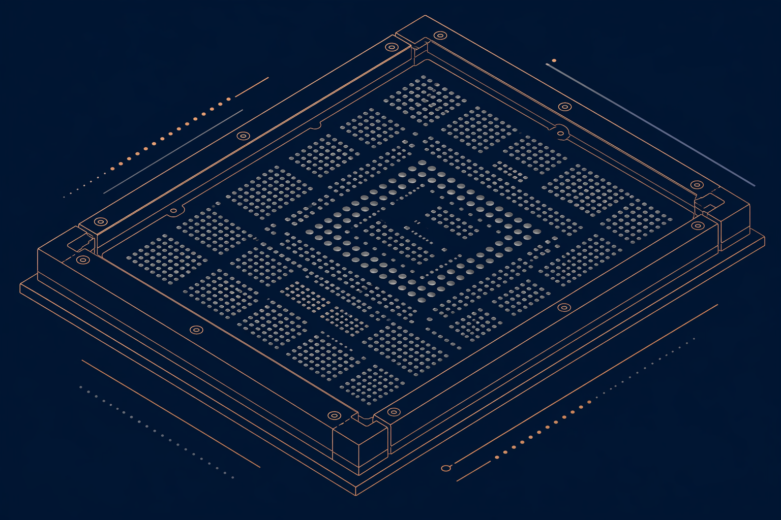
01005
Min Size

Complete single-board assembly integrating SMT, through-hole, press-fit, connector, and wire harness technologies. We manage process sequencing, thermal compatibility, and component clearance so you do not have to split your order.
Mixed-technology boards follow a strict SMT-first then DIP-second sequence. Each stage has defined entry criteria and inspection gates. The process is designed to protect SMT solder joints from thermal damage during DIP processing.
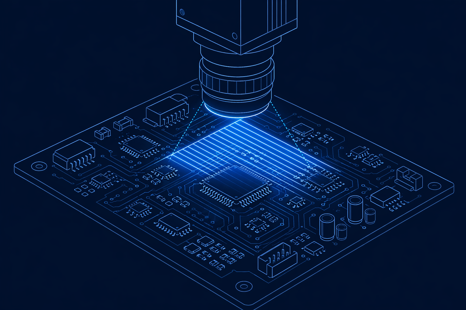
Laser-cut stainless steel stencil matched to SMT pad geometry only. Through-hole pad areas are masked. 3D SPI verifies paste deposit volume, area, and height on every SMT pad. The stencil design accounts for the fact that through-hole components will be inserted later and therefore must not interfere with SMT placement clearance.
All surface-mount components are placed first while the board is flat and unobstructed. Placement programs respect keep-out zones around future through-hole insertion areas to prevent collision risk. Vision-centering on every component from 01005 passives to 45 mm BGAs. Feeder setup verified against BOM before production begins.
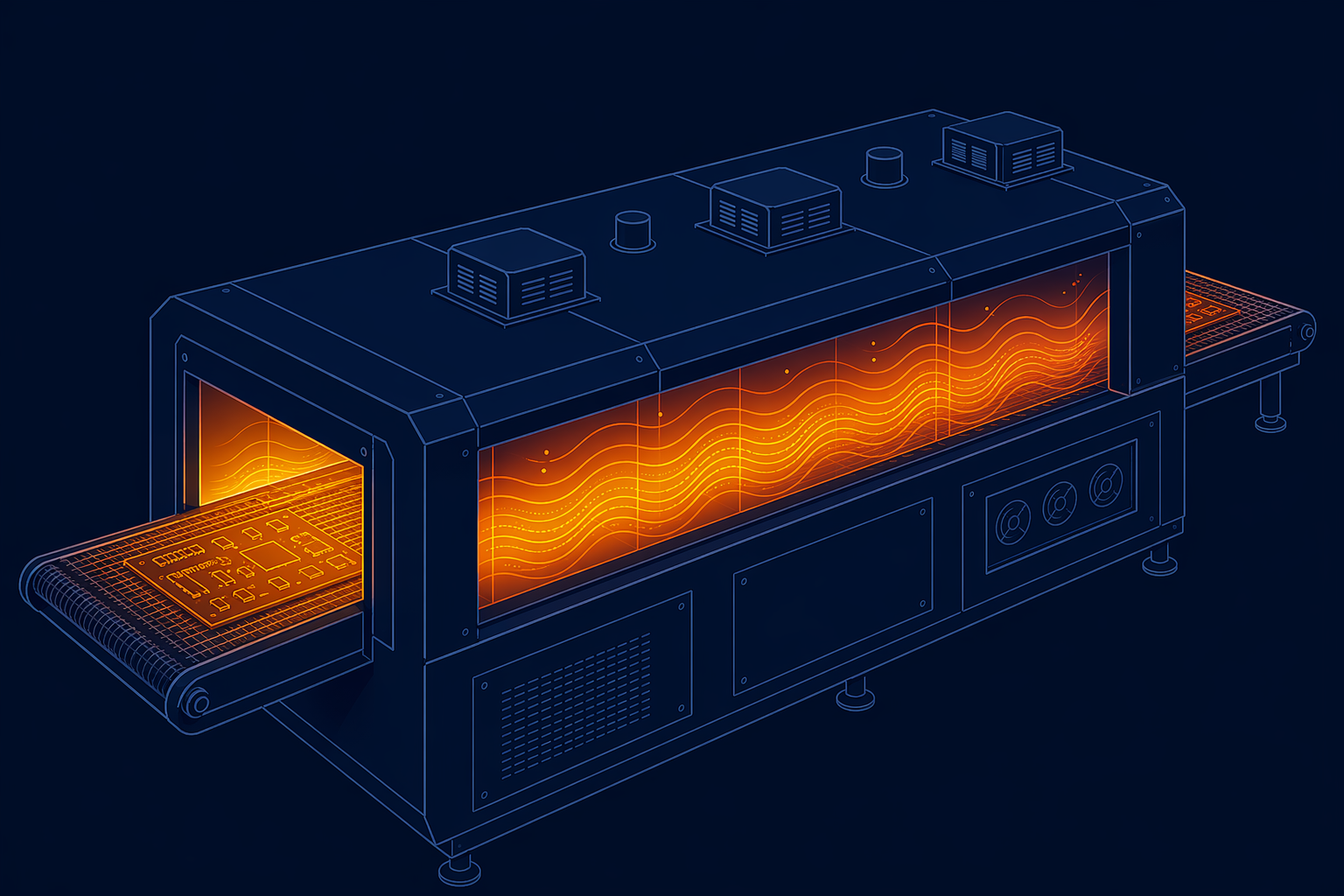
Twelve-zone reflow with a thermal profile designed for the full board mass including unpopulated through-hole pad areas. For boards with heat-sensitive through-hole components that cannot be installed after reflow, a shadow mask is used to shield designated areas from peak reflow temperature. Every thermal profile is board-specific and validated against the component set's J-STD-020 ratings.
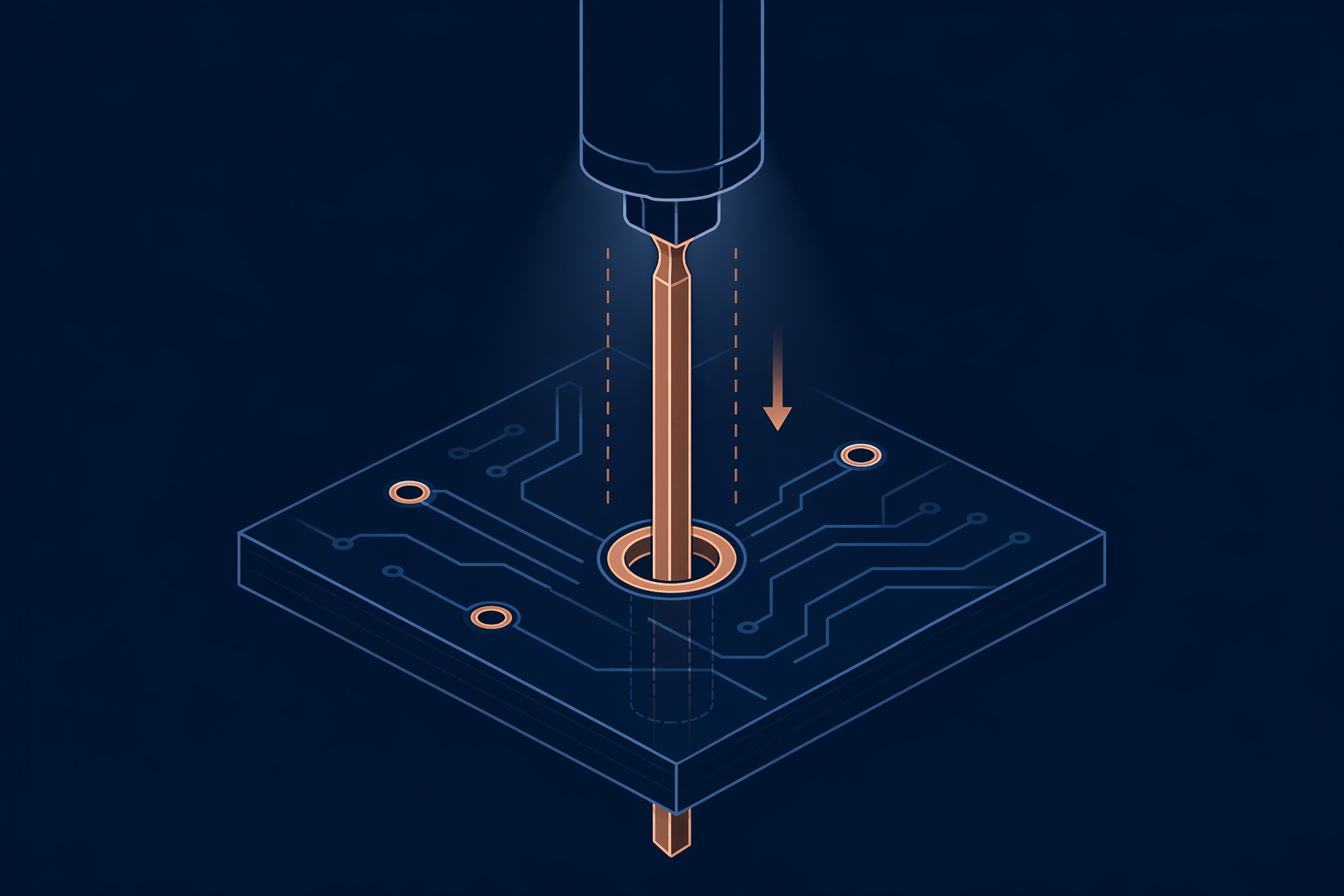
After the SMT side completes reflow and passes AOI, through-hole components are inserted. Axial, radial, DIP IC, connector, transformer, and odd-form components are placed using the appropriate insertion method for each type. Press-fit connectors are also installed at this stage. Components are kitted and verified per the BOM before insertion begins.
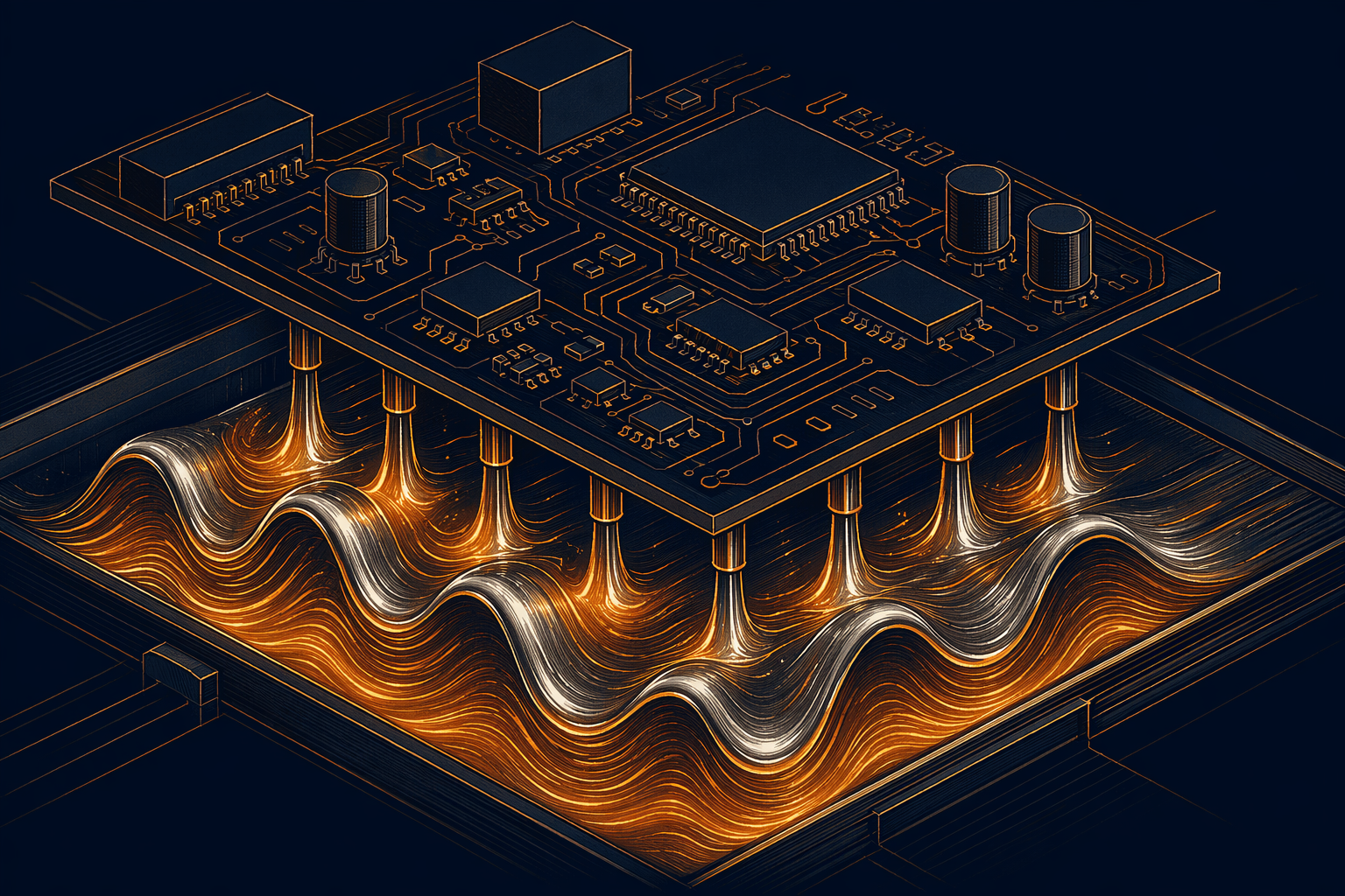
Through-hole soldering uses either full-board wave soldering or precision selective soldering depending on the board layout. Boards with SMT components on the bottom side require selective soldering to avoid re-melting existing SMT joints. SAC305 lead-free alloy throughout. The process temperature and dwell time are controlled to prevent thermal stress on already-reflowed SMT components on the opposite side.
Combined automated and visual inspection covering both SMT and DIP joints. AOI verifies SMT joint quality post-wave-solder thermal exposure. Manual 4× magnification inspection covers through-hole fill, fillet geometry, and wetting for every DIP joint. Connector mating surfaces and press-fit zones receive dedicated visual inspection for mechanical integrity.
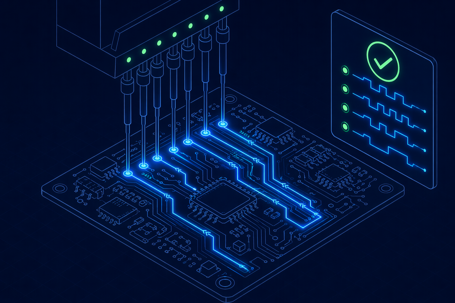
Full functional testing verifies the complete board after all SMT and DIP processing. Power-up sequence, signal integrity across both SMT and through-hole domains, boundary scan where applicable, and system-level functional verification against the test specification. Boards also undergo ICT if test points are available. A passing functional test is the final gate before the board is released for shipment.
Combined specifications reflect the full mixed-assembly line. The SMT-first, DIP-second sequence imposes no reduction in capability for either technology.
| Parameter | Specification |
|---|---|
| Mixed Technology Types | SMT + Through-Hole + Press-Fit + Connector + Wire Harness |
| Process Sequence | SMT first (reflow), then DIP (wave/selective) |
| Combined Max Board | 450 mm × 400 mm |
| Interconnect Methods | Press-fit + solder + connector mating |
| Thermal Management | Shadow mask for heat-sensitive through-hole near SMT reflow zones |
| Parameter | Specification |
|---|---|
| Min Component Size | 01005 (0.4 mm × 0.2 mm) |
| Max BGA Size | 45 mm × 45 mm |
| BGA Pitch Minimum | 0.3 mm |
| Placement Speed | 45,000 CPH |
| Parameter | Specification |
|---|---|
| Component Types | Axial, Radial, DIP IC, Connector, Transformer |
| Max Component Height | 70 mm |
| Insertion Methods | Manual, Semi-Auto, Full Auto |
| Soldering Methods | Wave (lead-free SAC305) + Selective |
Combining SMT and through-hole on one board introduces three fundamental challenges. Here is how we solve each one at the process level, not with workarounds.
The problem: SMT reflow reaches 235°C–250°C. Through-hole wave soldering exposes the bottom side to 245°C–265°C. Already-reflowed SMT joints on the bottom side can re-melt during wave soldering. Heat-sensitive through-hole components cannot survive the reflow profile if installed first.
Our solution: SMT is always processed first with all through-hole pads empty. For boards where through-hole components must be installed before reflow (mechanical reasons), we deploy a custom shadow mask — a stainless steel shield placed over heat-sensitive zones during reflow. During wave soldering, we use selective soldering instead of full-board wave when SMT components exist on the bottom side. This eliminates re-melt risk entirely. Every board gets a thermal simulation during the DFM review to identify potential conflicts before any physical processing begins.
The problem: Tall through-hole components (transformers, large capacitors, connectors up to 70 mm) crowd the board and block access for SMT placement nozzles and inspection cameras. Tightly packed mixed boards can have clearance violations that are invisible in CAD but catastrophic on the production line.
Our solution: During DFM review, we generate a 3D clearance map showing the keep-out volume around every component. Through-hole insertion is always sequenced after all SMT placement and reflow. If SMT components sit beneath or adjacent to tall through-hole parts, we verify that the SMT placement nozzle has physical clearance before committing to the build. For boards with extreme density, we provide a recommended insertion sequence that respects both thermal and mechanical constraints.
The problem: A mixed board can require five or more distinct process steps (SMT paste print, SMT pick-and-place, SMT reflow, DIP insertion, wave/selective soldering, inspection at multiple nodes). Each step demands different tooling, machine setup, and operator skillsets. Administrative errors in sequencing — running DIP before SMT, or skipping an inspection gate — can destroy an entire batch.
Our solution: Every mixed-technology board travels with a digital process traveler that enforces the manufacturing sequence. A barcode scan at each station validates that the previous step was completed and passed its inspection gate. The system physically prevents a board from being processed out of sequence — the wave solder machine will not accept a board whose SMT reflow and AOI records are not signed off. This is not an administrative procedure; it is built into the production execution system.
Mixed-technology boards pass through the full SMT and DIP equipment set. Every machine below is production-caliber and on the same factory floor.
Send us your design files for a free DFM review. We will map the process sequence, flag any clearance or thermal issues, and return a complete assembly quotation.