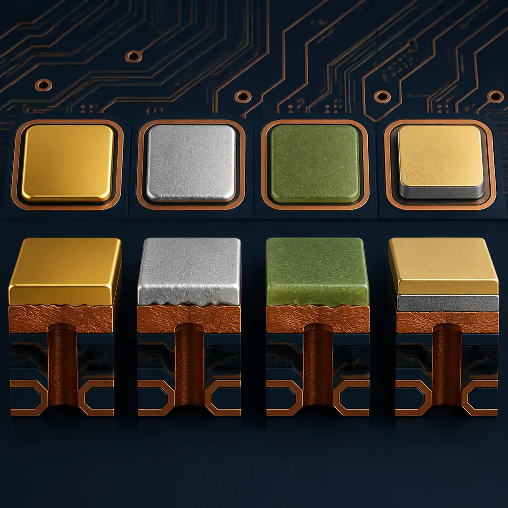
Every PCB fabrication order asks the same question: which surface finish? It's a deceptively simple choice that cascades through cost, assembly yield, shelf life, and long-term reliability. Pick the wrong finish and you might discover the problem 6 months later when boards stored in inventory refuse to solder — or 2 years later when ENIG black pad failures start appearing in the field.
The surface finish serves three jobs on every PCB pad: it protects the copper from oxidation before assembly, it provides a solderable surface for component attachment, and it influences the mechanical and electrical properties of the finished solder joint. A finish that excels at one of these jobs may be mediocre at the others — there is no universal "best" finish, only the right finish for your specific combination of component types, storage conditions, reliability requirements, and budget.
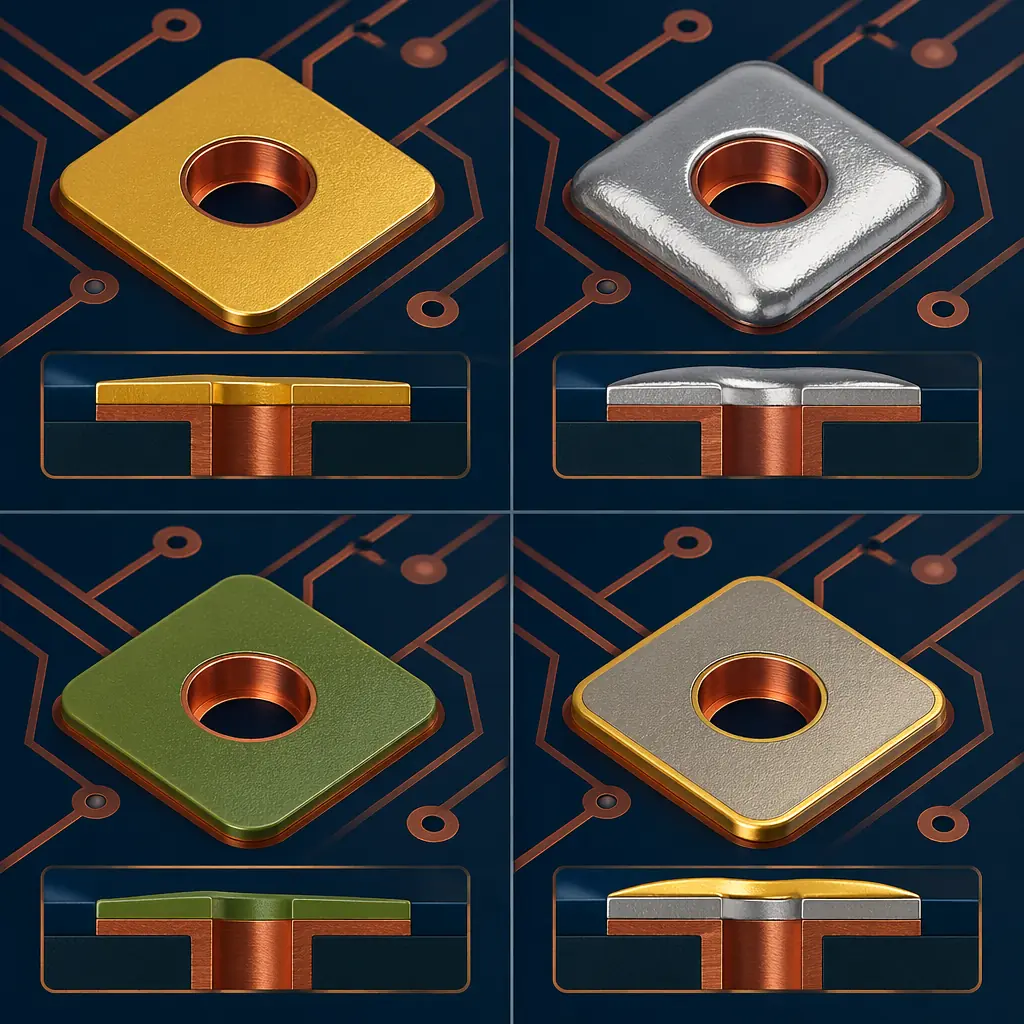
This guide compares the four most common PCB surface finishes — HASL, OSP, ENIG, and ENEPIG — across the dimensions that matter for procurement and engineering decisions: cost per square meter, flatness for fine-pitch components, shelf life in storage, solder joint reliability, and application fit. At Uppcba, we process all four finishes across our 6 SMT lines, and the data below draws from production experience across thousands of customer designs.
The Four Finishes at a Glance
| Property | HASL (Lead-Free) | OSP | ENIG | ENEPIG |
|---|---|---|---|---|
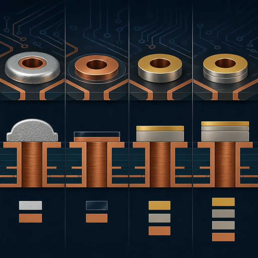
| Typical thickness | 1–40 μm (uneven) | 0.2–0.5 μm | Au: 0.05–0.12 μm Ni: 3–6 μm | Au: 0.05–0.12 μm Pd: 0.05–0.15 μm Ni: 3–6 μm |
| Flatness (coplanarity) | Poor — dome-shaped | Excellent — angstrom-level | Excellent — sub-micron | Excellent — sub-micron |
| Shelf life | 12+ months | 3–6 months | 12+ months | 12+ months |
| Cost (relative) | 1× (baseline) | 1.1–1.3× | 2.5–4× | 3.5–5× |
| Multiple reflow cycles | Good (but warping risk) | Poor — degrades after 1st pass | Excellent — 3+ passes | Excellent — 3+ passes |
| Wire bondable | No | No | Yes (Al wire) | Yes (Al + Au wire) |
| RoHS compliant | Yes (lead-free variant) | Yes | Yes | Yes |
HASL (Hot Air Solder Leveling): The Workhorse
HASL is the most widely used surface finish in PCB fabrication, and for good reason: it's the cheapest option, it's compatible with virtually all assembly processes, and it provides the longest shelf life of any finish — boards can sit in storage for over a year and still solder perfectly. The process dips the fabricated PCB into molten solder (tin-copper or tin-silver-copper for lead-free), then uses hot air knives to blow excess solder off the pads, leaving a solder-coated surface.
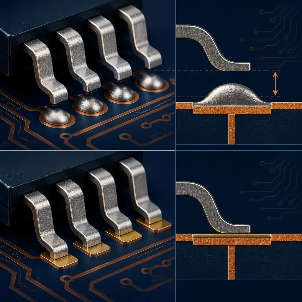
The flatness problem is HASL's primary limitation. The hot air leveling process cannot produce a perfectly flat surface — pads end up with a characteristic dome shape, with the solder thicker in the center and thinner at the edges. For 0603 passives, SOIC packages, and through-hole components, this dome is invisible to the assembly process. For 0.5 mm pitch QFPs and 0.8 mm pitch BGAs, the uneven surface creates coplanarity issues: some pads make solid contact with the solder paste and component leads, while others barely touch. The result is inconsistent solder joint formation and increased defect rates on fine-pitch components.
As a rule of thumb, HASL is reliable down to approximately 0.65 mm pitch for QFP packages and 1.0 mm for BGA. Below these thresholds, the coplanarity variation exceeds what the solder paste deposit can compensate for, and yield drops measurably. For designs with 0201 passives or 0.5 mm pitch ICs, HASL should be replaced with a flat finish — OSP for cost-sensitive applications, or ENIG/ENEPIG when shelf life and multiple reflow cycles are required.
When to choose HASL
- Component pitch ≥ 0.65 mm (QFPs, SOICs, 0603+ passives)
- Boards that may sit in inventory for 6+ months before assembly
- Cost-sensitive consumer and industrial products
- Through-hole-heavy designs where flatness is irrelevant
OSP (Organic Solderability Preservative): Budget Flatness
OSP applies a water-based organic compound to the copper pads that forms a thin (0.2–0.5 μm), transparent protective layer. Unlike HASL, OSP adds essentially zero thickness variation — the surface remains as flat as the bare copper pad beneath it. This makes OSP the budget choice for fine-pitch designs: you get ENIG-level flatness at roughly one-third of the cost.
The shelf life trade-off is where OSP shows its limitations. The organic coating gradually degrades when exposed to humidity and elevated temperatures. In a controlled environment (20–25°C, <60% RH, sealed packaging), OSP-coated boards typically remain solderable for 3–6 months. In uncontrolled storage — a hot warehouse in Southeast Asia, for example — shelf life can drop below 3 months. After the OSP layer degrades, the exposed copper oxidizes, and the board requires either a bake-out and re-application or scrapping.
Multiple reflow vulnerability is OSP's other major constraint. The first pass through reflow burns off the organic coating, leaving bare copper on the unsoldered pads. If your board requires a second reflow pass — common in double-sided SMT assemblies where the bottom side is assembled first, then the top side — those bottom-side pads have no protection between passes. The copper begins oxidizing immediately, and the second-pass solder joint quality depends on the flux in the solder paste being aggressive enough to clean the oxidized copper. For single-sided assemblies, this is a non-issue; for double-sided SMT, it adds process risk that can show up as intermittent wetting defects. For deeper guidance on preparing your design for SMT, see our DFM preparation guide.
When to choose OSP
- Fine-pitch designs (≤0.5 mm QFP, <1.0 mm BGA) on a budget
- Single-sided SMT assemblies (no second reflow pass)
- Boards that will be assembled within 3 months of fabrication
- Controlled storage conditions available (sealed packaging, climate control)
ENIG (Electroless Nickel Immersion Gold): The Industry Standard for Reliability
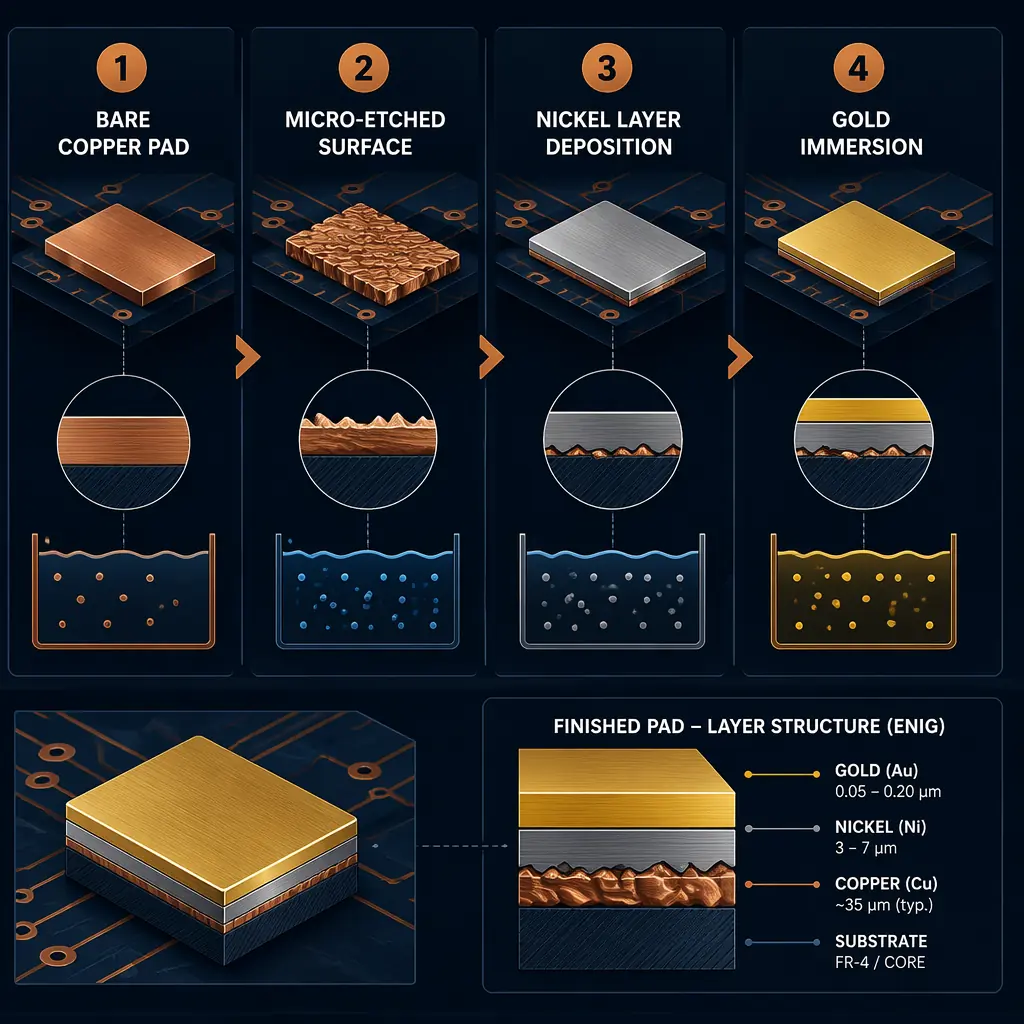
ENIG is the most widely specified flat surface finish for professional and high-reliability applications, and it earns its position through a rare combination of properties: excellent flatness, 12+ month shelf life, multiple reflow cycle tolerance, and good electrical contact performance. The process deposits a layer of electroless nickel (3–6 μm) directly onto the copper pad, followed by a thin immersion gold layer (0.05–0.12 μm) that protects the nickel from oxidation. At Uppcba, ENIG is the default finish we recommend for IPC Class 3 assemblies unless a specific application requirement dictates otherwise.
The cost reality: ENIG costs 2.5–4× more than HASL per square meter of board area. On a typical 100 × 100 mm board, the finish cost adder is roughly $1.50–$3.00 — modest in the context of a $30–$80 assembly bill. Where the cost becomes material is on large boards (200 × 200 mm or more), where the finish adder can reach $10–$15 per board. For high-volume consumer products, this difference matters. For medical devices, aerospace, and industrial control systems where a field failure costs orders of magnitude more than the finish premium, ENIG is the standard choice.
Black pad syndrome is the failure mode that has given ENIG its one well-known vulnerability. Black pad occurs when the immersion gold plating process over-reacts with the nickel layer, creating a phosphorus-rich, brittle nickel-phosphide interface that fractures under mechanical or thermal stress. The solder joint appears to have wet properly — the solder ball sits on the pad — but the intermetallic bond is weak, and the joint separates at the Ni-P interface, leaving a characteristic dark gray or black fracture surface. Black pad is a process control problem at the PCB fabricator, not an inherent ENIG flaw. Reputable fabricators control immersion time, gold bath temperature, and pH within tight windows that prevent the over-reaction. When evaluating a PCB supplier, ask about their phosphorus content control in the nickel bath — it should be maintained at 6–9% by weight, verified by bath analysis at least once per shift.
When to choose ENIG
- Fine-pitch SMT: 0201 passives, 0.4–0.5 mm pitch BGAs, QFNs
- Boards requiring 2+ reflow passes (double-sided SMT)
- Long shelf life required (6+ months between fab and assembly)
- IPC Class 3 / high-reliability applications (medical, aerospace, automotive)
- Contact surfaces: keypad contacts, edge connectors, test points
ENEPIG (Electroless Nickel Electroless Palladium Immersion Gold): When ENIG Isn't Enough
ENEPIG adds a middle layer — electroless palladium (0.05–0.15 μm) — between the nickel and gold layers of ENIG. This palladium layer acts as a diffusion barrier that prevents the nickel from migrating into the gold during storage and thermal cycling, solving two ENIG limitations simultaneously: it eliminates the phosphorus enrichment that causes black pad, and it makes the surface wire-bondable with both aluminum and gold wire, whereas ENIG only supports aluminum wire bonding reliably.
The cost premium over ENIG is significant — roughly 40–60% more — because palladium is an expensive platinum-group metal and the process adds an extra plating step. On a per-board basis, ENEPIG adds $2–$5 over ENIG for a typical 100 × 100 mm board. This premium is hard to justify unless your application specifically needs wire bonding capability, ultra-long storage life (>2 years in uncontrolled conditions), or the absolute elimination of black pad risk in high-reliability applications where failure is not an option — implantable medical devices, satellite electronics, or downhole oil-and-gas instrumentation.
For the vast majority of PCB assembly applications — including medical devices at the system level, industrial controls, and automotive electronics — ENIG provides sufficient reliability margin. ENEPIG enters the conversation when your reliability engineer asks for it by name, which typically means they've experienced a black pad failure on a previous design or they're working to a specification (MIL-PRF-31032, NASA-STD-8739) that mandates nickel barrier integrity verification beyond standard ENIG process control.
When to choose ENEPIG
- Wire bonding required (Au or Al wire) — especially mixed wire bond + SMT designs
- Absolute black pad elimination required (implantable medical, space-grade)
- Extreme storage conditions: >2 years shelf life or uncontrolled tropical environment
- High-temperature applications where Ni-Au intermetallic growth is a concern
Selection Matrix: Match the Finish to Your Application
| Application | Recommended Finish | Acceptable Alternative | Avoid |
|---|---|---|---|
| Consumer electronics, ≥0603, single-sided | HASL | OSP | ENEPIG (overkill) |
| Consumer electronics, fine-pitch, double-sided | ENIG | OSP (if assembled within 3 months) | HASL (coplanarity issues) |
| Industrial controls, 5–10 year life | ENIG | — | OSP (shelf life risk on spares) |
| Medical devices, non-implantable | ENIG | — | HASL, OSP |
| Implantable medical, space-grade | ENEPIG | ENIG (with black pad process audit) | HASL, OSP |
| Automotive under-hood, -40 to +125°C | ENIG | ENEPIG | OSP (thermal degradation) |
| Prototype / proof-of-concept, fast turn | HASL | ENIG | ENEPIG (cost, lead time) |
| RF / microwave, controlled impedance | ENIG | OSP | HASL (uneven surface affects impedance) |
How Surface Finish Affects DFM and Assembly Yield
Your choice of surface finish interacts with several DFM decisions, and understanding these interactions prevents yield surprises at the assembly stage. Three specific interactions deserve attention:
Stencil design and solder paste volume: HASL pads, because of their dome shape, effectively reduce the standoff height between the stencil and the pad surface. The stencil does not sit completely flat on a domed HASL pad — it contacts the center of the dome, leaving a small gap at the pad edges. This gap allows solder paste to bleed under the stencil at the pad perimeter, producing a slightly larger paste deposit than designed. For designs transitioning from HASL to ENIG, the paste volume should be re-verified — the same stencil aperture that produced good joints on HASL may under-deposit on perfectly flat ENIG pads because the gasketing effect of the dome is gone.
Component placement force: Fine-pitch BGAs (0.5 mm and below) require a flat landing surface because the solder ball collapse height is only 200–300 μm. On a domed HASL pad, a BGA ball may contact the center of the dome before the perimeter balls make contact, creating uneven collapse and potential opens on the outer rows. ENIG and OSP eliminate this variable entirely, which is a major reason they're specified for fine-pitch BGA designs. Our DFM guide covers these interactions in detail.
ICT (in-circuit test) probe contact: Test pads and vias used as test points need a surface that makes reliable electrical contact with spring-loaded pogo pins. ENIG provides consistently low contact resistance because the gold surface does not oxidize. HASL test pads develop a thin oxide layer over time that can cause intermittent contact — particularly on boards tested weeks after assembly. If your test strategy includes ICT, specify ENIG at minimum on test pads, or budget for double-probing (two pins per net) on HASL boards.
Procurement Checklist: Questions to Ask Your PCB Fabricator
When specifying a surface finish, the spec sheet tells you what the fabricator aims to produce. These five questions tell you what they actually control:
| # | Question | What to Look For |
|---|---|---|
| 1 | "What is your nickel bath phosphorus content and how often do you analyze it?" | 6–9% P by weight; analyzed at minimum once per shift. Outside this range = black pad risk. |
| 2 | "Do you perform solderability testing on every batch, and to which standard?" | IPC J-STD-003, wetting balance or dip-and-look method. Certificate should reference the standard. |
| 3 | "What is your maximum time between OSP application and vacuum packaging?" | Under 2 hours. OSP begins degrading on exposure to ambient humidity. |
| 4 | "Can you provide XRF thickness measurements for the Au, Pd, and Ni layers?" | XRF report should show all layer thicknesses within spec. Au below 0.03 μm = porosity and oxidation risk. |
| 5 | "Do you have experience with [your specific finish] on [your layer count and thickness]?" | Specific, not generic. A fabricator who's done ENIG on 2-layer 1.6 mm may not have the thermal management for ENIG on 12-layer 2.4 mm. |
The Bottom Line: Pick for Your Hardest Component, Not Your Average
The most common surface finish mistake we see at Uppcba is choosing based on the majority of components rather than the most demanding one. A board with 200 0603 resistors and one 0.5 mm pitch BGA should be specified for the BGA, not the resistors. Saving $2/board on HASL for the 200 easy components and then fighting BGA coplanarity defects at 2% yield loss on every production run is a false economy that the procurement spreadsheet won't show you — but the rework station operator will.
When you're ready to specify a surface finish for your next design, the same evaluation framework you use for choosing an assembly partner applies here: define your hardest requirement first (finest pitch, most reflow cycles, longest shelf life, highest reliability standard), then select the least expensive finish that satisfies it. This approach, consistently applied, produces better assembly outcomes than optimizing for cost alone — a principle that holds true across every manufacturing decision in PCB assembly.
Surface finish is one of several material choices that affect your assembly lead time — ENIG and ENEPIG add 1–2 days to PCB fabrication compared to HASL, which matters when you're working to a tight schedule. Factor this into your planning timeline from the start rather than discovering it after the PCB order is placed.