PCB Manufacturing
Precision PCB Fabrication
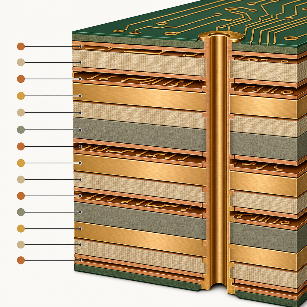
2–32 layers. 2.5/2.5 mil trace/space. HDI any-layer. 80,000㎡ monthly capacity.
2–32 layers. 2.5/2.5 mil trace/space. HDI any-layer. 80,000㎡ monthly capacity.
| Parameter | Standard Capability | Advanced Capability |
|---|---|---|
| Layer Count | 2-16 layers | 18-32 layers |
| Board Thickness | 0.4mm - 3.2mm | 0.2mm - 6.0mm |
| Min Trace / Space | 4/4 mil | 2.5/2.5 mil (HDI) |
| Min Hole Size (Mech) | 0.25mm | 0.15mm |
| Min Hole Size (Laser) | 0.10mm | 0.075mm |
| Impedance Control | ±10% | ±5% (premium ±3%) |
| Copper Weight | 1oz - 3oz | 0.5oz - 12oz |
| Aspect Ratio | 10:1 | 16:1 |
| Solder Mask Color | Green, Blue, Red, Black, White, Yellow, Purple, Matte Green, Matte Black | |
| Silkscreen | White, Black, Yellow | |
| Min BGA Pad | 0.35mm | 0.25mm |
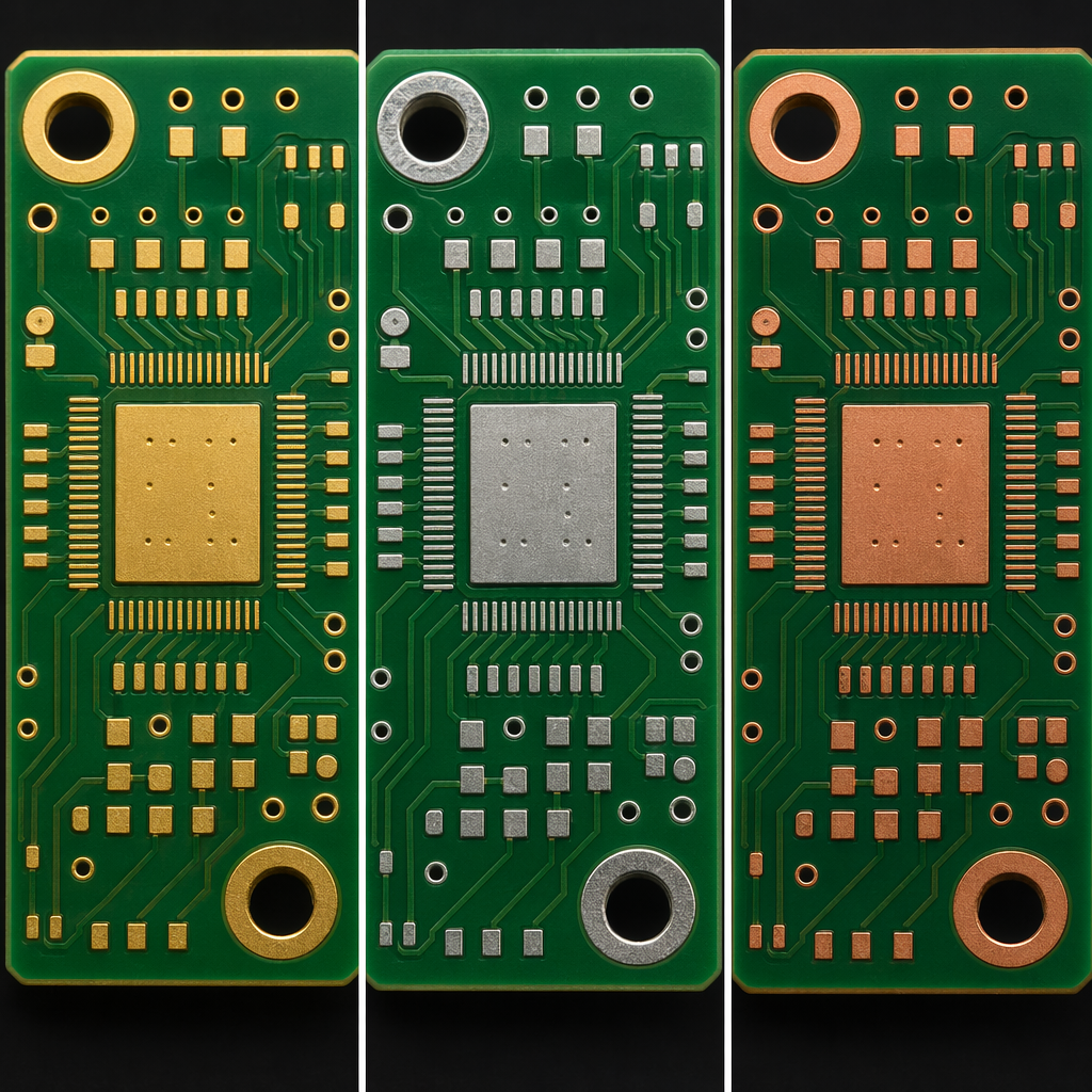
Gold over Nickel — best solderability, flat surface
Gold over Palladium over Nickel — wire bonding
Tin-Copper-Silver — RoHS compliant, cost-effective
Silver coating — RF/high-frequency, smooth surface
Tin coating — fine pitch, flat pads
Organic coating — cost-effective, RoHS, short shelf life
Thick gold — edge connectors, high durability
Tin-Lead — legacy applications, excellent solderability
Standard FR-4 to advanced high-frequency laminates.
Upload your Gerber files. Free DFM check. Quote within 24 hours. Prototype in 3 days.
Get PCB Quote →