
When you submit a PCB assembly order, the first question every procurement manager asks is: "When will it be ready?" The answer depends on more than just how many boards you need. Component availability, stencil fabrication, inspection requirements, and even the time of month can shift your delivery date by days or weeks. Understanding what drives those variables — and where you can influence them — turns an unpredictable timeline into a manageable schedule.
At Uppcba, we assemble boards for clients across 18 countries, from 5-piece prototypes to 5,000-unit production runs. We've seen the same lead-time patterns repeat across hundreds of projects. Here are the six factors that consistently make the difference — and what you can do about each one.
1. Component Availability Is the Dominant Variable
Over 60% of assembly delays trace back to one issue: components not being in stock when the production slot opens. A design calls for a specific voltage regulator that has a 12-week lead time from the manufacturer; your assembly partner discovers this only after receiving the BOM; the entire schedule slides. This is the most common, most expensive, and most preventable cause of production delay.
The fix starts before you send the BOM. For every part that is not a generic passive — resistors, capacitors below 1 µF, standard diodes — designate at least one approved alternate with verified current stock at a major distributor. Specify both the primary and alternate manufacturer part numbers on the BOM. When your assembler sees that the primary is unavailable, an experienced team will immediately pivot to the alternate rather than stopping the line and sending an email requesting direction. That email exchange — send, wait, reply, approve — costs 1 to 3 business days every time it happens, and it happens on roughly 40% of first-submission BOMs.

2. Stencil Tooling: The Hidden 48-Hour Gate
Every SMT assembly job requires a solder paste stencil — a laser-cut stainless steel foil, typically 0.1 mm to 0.15 mm thick, with apertures that match your board's pad geometry. Stencil fabrication is not instant. A standard laser-cut stencil takes 24 to 48 hours from Gerber data receipt to finished tool, longer if the design requires a step stencil for mixed fine-pitch and power-component applications.
This lead time is fixed and non-negotiable. No assembler can start placing components before the stencil is ready. Where you can influence the timeline is by submitting Gerber files that are stencil-ready — meaning pad geometries are standard, paste mask layers are included in the Gerber package, and no last-minute layout changes arrive after stencil fabrication begins. A stencil remade mid-project costs another 24 to 48 hours plus the tooling charge. Our engineering team provides a stencil design review as part of the standard DFM check before committing to production.
3. Batch Size and Line Scheduling
Assembly lines operate on production slots. A 5-board prototype run consumes a different slot than a 500-board production batch, and the scheduling logic is not linear. A prototype that requires 30 minutes of setup and 10 minutes of placement time might slot into a morning gap. A production run that requires 3 hours of continuous placement time needs a dedicated afternoon block. If you miss the morning slot, your boards wait until the following day.
The practical takeaway: submit orders with realistic quantities. Ordering "5 prototypes now, 500 later" is a valid strategy, but treat them as two separate production events with two separate lead-time commitments. Combining them into a single order that changes quantity mid-process is what creates scheduling chaos. And be aware that quarterly-end rushes can add 3 to 5 business days to standard lead times across the industry.
4. Inspection Requirements: AOI, X-Ray, and Functional Test
Not all inspection is created equal. AOI adds approximately 2 to 5 minutes per board and is performed inline — it does not typically extend the overall lead time. X-ray inspection for BGA and QFN packages, however, is a batch process performed on a separate station. A run of 200 boards with BGA inspection adds 3 to 4 hours of dedicated X-ray time, which may need to be scheduled outside of peak line hours.
Functional test requires a custom test fixture and a test program. Fixture fabrication alone takes 3 to 5 business days if it does not already exist. If you are ordering a first-run prototype without an existing test fixture, factor that lead time into your schedule explicitly. Our team can design and build a test fixture concurrently with stencil fabrication, provided we receive the test specification at the same time as the Gerber data.
Specify your inspection requirements clearly on the assembly drawing. Vague instructions like "test to ensure functionality" generate clarification emails and schedule delays. "Verify output voltage 5.0 V ± 0.1 V under 2 A load at test points TP1 and TP2, record value per serial number" is an instruction that the line can execute immediately.

5. Mixed-Technology Boards: The Through-Hole Factor
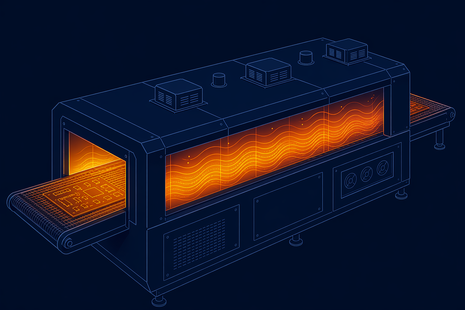
A pure SMT board moves through a single automated process: paste print, place, reflow, AOI. A mixed-technology board requires a second process step: wave soldering or selective soldering for the through-hole parts, performed after the SMT reflow cycle is complete.
Wave soldering adds roughly 30 to 60 minutes of additional process time per batch, plus fixture loading time. Selective soldering is slower per board but eliminates fixture setup time. Fewer than 10 through-hole components per board: selective soldering is faster overall because it skips fixturing. More than 20: wave soldering wins on throughput.
The lead-time impact of mixed technology is largely fixed — you cannot eliminate the second process step. What you can control is fixture readiness. Uppcba maintains an in-house fixture workshop that can turn around a standard wave pallet in 48 hours, provided we have the board outline data.
6. Documentation Completeness: The Paperwork Tax
An assembly order is not complete when you send the Gerber files. It is complete when the assembler has Gerber data, BOM with approved alternates, CPL file with coordinates and rotations, an assembly drawing, any test specification, and — if applicable — a conformal coating mask drawing. Missing any one of these triggers a request-for-information cycle that adds 1 to 3 days per missing item.
The most commonly missing items are the CPL file and the assembly drawing. A CPL file that uses a different board origin than the Gerber data is functionally the same as no CPL file. Verify that your ECAD tool exports the CPL in the same coordinate system as your Gerber output. This single check eliminates roughly 15% of all production delays we encounter.
Realistic Lead Time Benchmarks
Based on our production data across 500+ projects, here is what you can expect for standard PCB assembly turnaround under normal conditions — all components in stock, documentation complete, no fixture fabrication required:
| Project Type | Typical Turnaround |
|---|---|
| Prototype (5–20 boards, SMT only) | 3–5 business days |
| Prototype (5–20 boards, mixed technology) | 5–7 business days |
| Low-volume production (100–500 boards, SMT only) | 7–10 business days |
| Low-volume production (100–500 boards, mixed tech) | 10–14 business days |
| Mid-volume production (500–5,000 boards) | 14–21 business days |
| With functional test fixture fabrication | Add 3–5 business days |
| With wave solder fixture fabrication | Add 2 business days |
Conclusion: Lead Time Is a Design Variable, Not a Given
The single most effective way to compress your PCB assembly lead time is to submit a complete package on the first try. Gerber data, BOM with alternates, CPL with verified coordinates, assembly drawing with orientation notes, and inspection requirements stated explicitly. When that package arrives at Uppcba, our engineers can begin stencil fabrication and component kitting on the same day.
If you plan to move into production within the next quarter, submit your design for a free DFM review now. Our engineering team will identify every lead-time variable in your specific design before you commit to a production schedule. That review costs nothing and can compress your final delivery date by days or weeks.