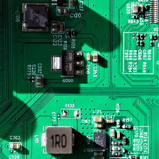
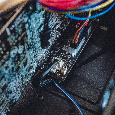
Top Custom PCB Board
Manufacturer from China
High-quality, high-performance printed circuit boards, regardless of
complexity or scale, tailored to your specs.
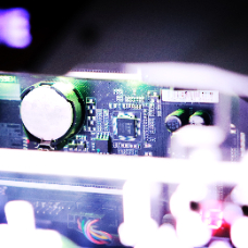
Your one-stop PCB source: explore our multilayer,
HDI, specialized options, and more.

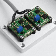
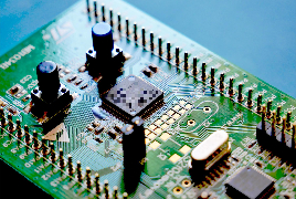
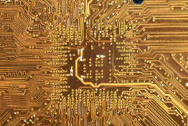
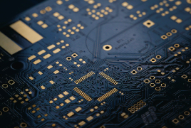
Designed for complex circuits requiring high functionality in compact spaces, ensuring reliability and superior signal integrity.

Combine flexibility with structural integrity, perfect for dynamic environments, offering streamlined packaging and enhanced connection reliability.

Choose our Aluminium PCBs for high-power applications. Known for excellent heat dissipation, they ensure longevity and stability in LED lighting and power circuits.

Tailored for applications demanding durability and adaptability, offering exceptional conformability and resistance to vibrations and heat.

Opt for our HDI PCBs when precision is key. With fine features and high-density components, they are ideal for advanced electronics requiring miniaturization without compromising performance.
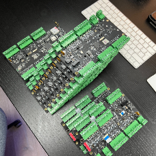
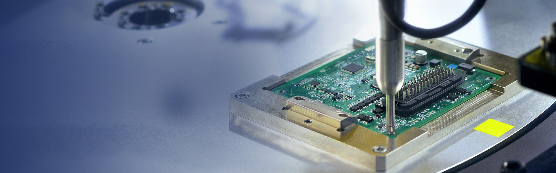
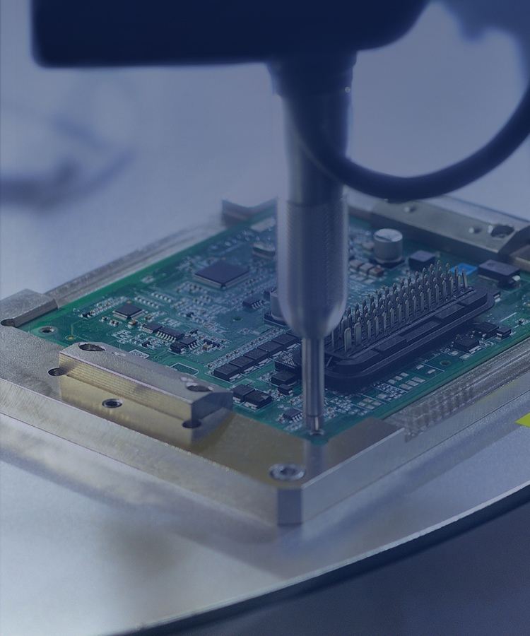
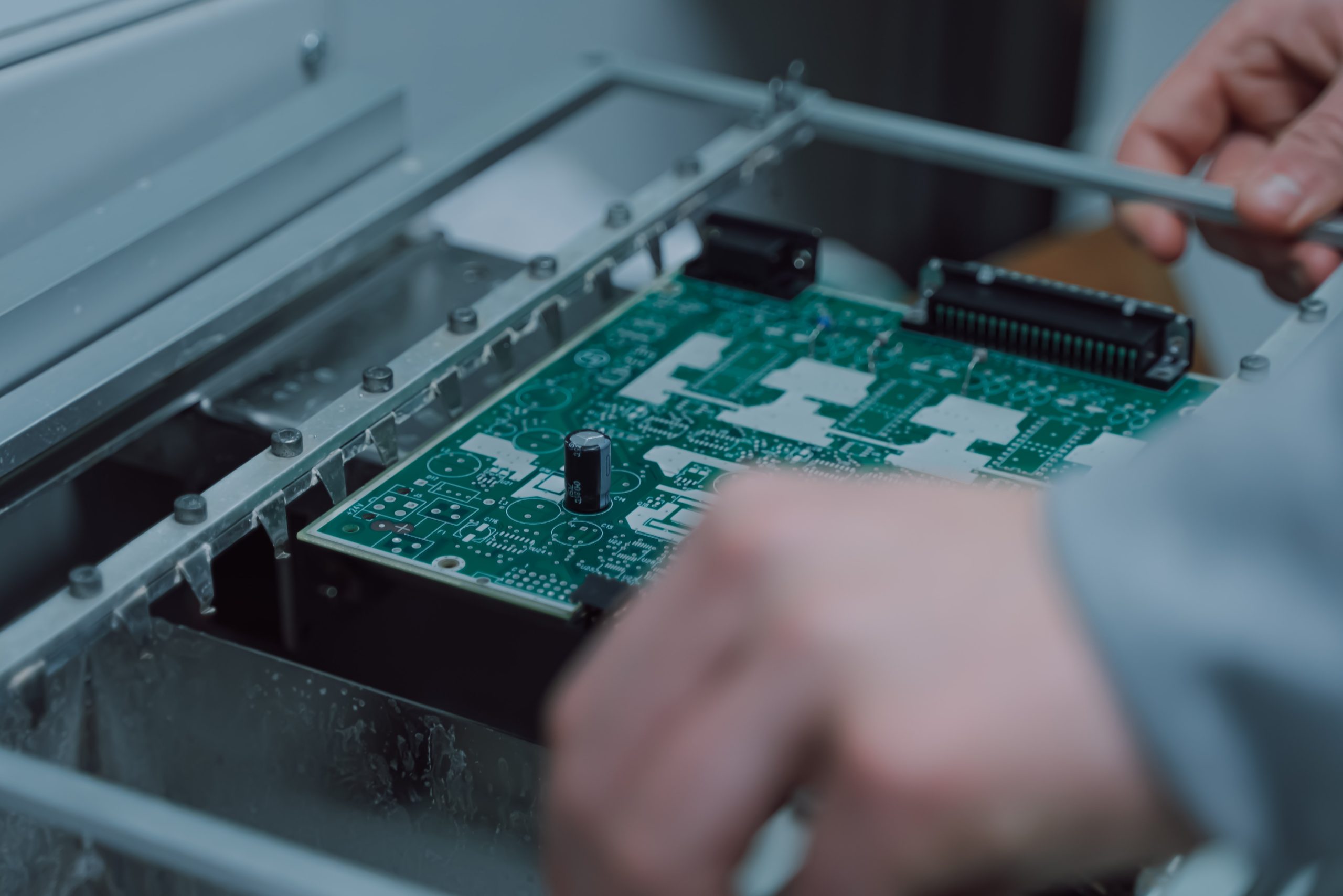
We Turn Complex Components
into Elegant Products
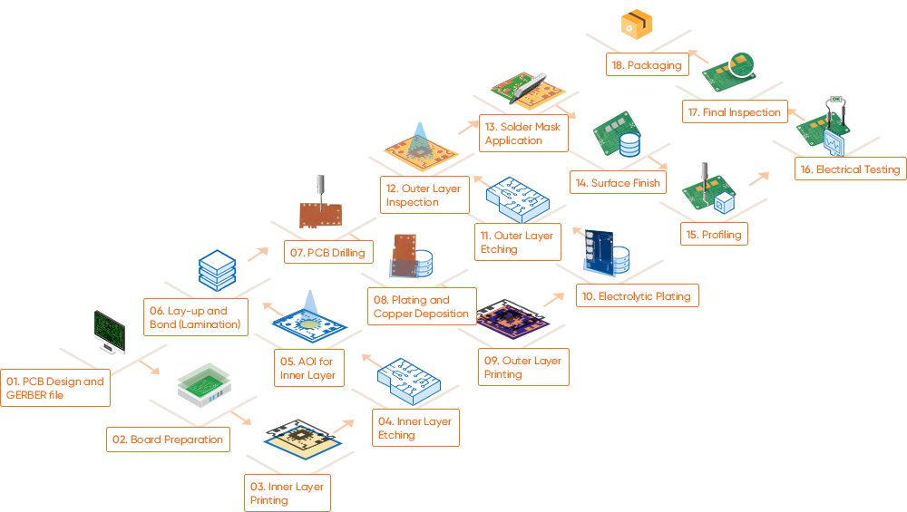
Upload your manufacturing data, typically in the form of Gerber files, which are standard for PCB production, detailing every aspect of the board’s design.
The base material, usually a type of fiberglass like FR4, is prepared by cutting it to the required size. This material forms the substrate of the PCB.
Copper is then laminated onto this substrate to create a conductive surface where the circuit will be etched.
A photoresist, a light-sensitive material, is applied to the copper layer. The PCB design is then printed onto a transparent film and placed over the material. Exposing it to UV light hardens the photoresist where the circuit should be, leaving other areas soft for removal
The inner layers are layered together with an insulating material known as pre-preg. Oxide layers are applied for better adhesion, and copper foil is added to the top and bottom. The stack is then subjected to high temperature and pressure to bond the layers into a solid structure.
After etching, the inner layers are scanned to compare the actual etched circuit against the intended design. This Automated Optical Inspection checks for any discrepancies, ensuring the circuitry is accurate and free of defects. Any anomalies detected are examined by trained inspectors.
The unhardened photoresist is washed away, exposing the bare copper, which is then removed chemically, leaving the hardened photoresist-protected copper circuit in place. This step carves out the pathways for the electrical circuit on the PCB by removing the unwanted copper.
Holes are precisely drilled into the stacked board for mounting components and creating vias (electrical connections between different layers). This is done with high-speed automated drills, guided by the board’s design files to ensure accuracy.
The drilled holes are plated with copper to create conductive pathways through the board. This process involves electroplating, where the entire board is submerged in a copper-plating bath, allowing copper to deposit into the drilled vias, establishing a connection between the layers.
Transfer the intended circuit pattern onto photosensitive dry film laminated onto the outer copper layers in a cleanroom environment. Selectively expose the dry film to ultraviolet light through the circuit artwork film. Then chemically develop it by dissolving away the unexposed dry film, while hardened exposed film protects areas of copper that will become tracks and pads.
Use automated optical inspection and x-ray laminography to verify the outer layer circuitry features like line widths, annular rings, spacing match the digital design and meet quality requirements.
Remove the outer layer copper not protected by the tin etch-resist using an ammoniacal etchant solution. Then chemically strip away the tin barrier layer using an alkaline solution without attacking the underlying copper conductors.
Electroplate a thicker layer of copper, around 1 oz (35 μm), onto the outer layer copper that is no longer protected by dry film, to build up the final thickness of conductors. Then electroplate a thin layer of tin (around 0.5-0.7 μm) onto the copper as an etch-resist barrier. Strictly control the plating bath chemistry, current density, temperature, etc. to deposit uniform and continuous layers with good adhesion.
Laminate a negative-acting epoxy solder mask layer onto the PCB outer surfaces. Use the solder mask artwork film to block UV light during exposure everywhere except solderable metal pads and features that must remain uncoated. Solvent develop to remove the unexposed, uncured solder mask.
Apply metal coatings like ENIG (electroless nickel immersion gold) or immersion tin onto exposed copper pads and features to protect against oxidation and improve solderability. Verify thickness and solder leaching resistance meet specs.
Cut or rout the panelized PCBs down to individual board dimensions based on the customer’s designs. Deburr edges and confirm conformance to all dimensional tolerances.
Wrap finished boards after inspection in antistatic and moisture barrier materials then pack securely into shipping containers. Label boxes indicating appropriate transport and storage requirements to destinations.
Perform careful detailed visual inspection of boards and statistically sample product to confirm adherence to workmanship quality and acceptance criteria standards.
Test for short and open circuits by checking continuity of circuits between test points. Validate correct connectivity between component pins and compliance with maximum net impedance through fixtures or flying probes.
Benefit from Our Advanced
PCB Manufacturing Techniques
Start a collaboration that seamlessly blends affordability, flexibility,adaptability, and
the efficiency of factory-direct access.
From simple 2 layer boards up to complex 64+ layer stacks. More layers allows for more complex routing.
Our manufacturing processes reliably produce ultra-fine 3mil traces and spaces, enabling intricate and spacious layouts.
Plated through hole, microvias, buried and stacked vias, leveraging seamless interconnection to facilitate layer transitions in multilayer designs.
Lead-free HASL, immersion gold(ENIG), immersion silver, immersion tin, OSP, hard gold, solderplating, etc.
Our capabilities extend to custom solder mask and silkscreen colors for clear labeling, backed by stringent testing methods like AOI and X-ray for quality assurance.